Nowadays it’s almost taken for granted that lasers are extremely fast and extremely precise. Essentially it’s true, because lasers really do offer extreme speed and precision—but only if correspondingly precise optics can be produced at a reasonable price. So far, that has always been the case, so lasers have managed to keep pace with whatever ideas users could come up with.
More space thanks to a narrower cut
The problem is that these ideas are becoming increasingly ambitious. In microelectronics, for example, there is more and more interest in using ultrashort pulse lasers instead of diamond wafer saws. The reasoning is that this could distinctly increase the usable surface area of a wafer of LEDs. With its precise focusing capabilities, a laser gets the job done by cutting a gap measuring less than 20 micrometers.
And because lasers work with micrometer precision and have very little effect on the edges, you can theoretically make do with a smaller safety margin on the edges of each LED. That makes the LEDs smaller and means you can fit more of them on the same wafer surface. What’s more, a scanner solution with multiple beams working in parallel can operate ten times faster than a mechanical saw.
That’s the theory anyhow. The trouble is that just as users’ and researchers’ interest in this new kind of process began to grow a few years ago, so too did the number of question marks hanging over it. One of the initiatives set up to tackle these uncertainties was the Semilas joint research project funded by Germany’s Federal Ministry of Education and Research.
The aim of the project was to develop an industrial process and provide the technical basis for a suitable system. As well as Osram, the mechanical engineering company Kugler, Topag—a manufacturer of diffractive optical elements (DOE) such as beam splitters—and a laser manufacturer, the project also drew on the specialist skills of the precision optics firm Ingeneric. And that’s because the optics component represented one of the biggest question marks of all.
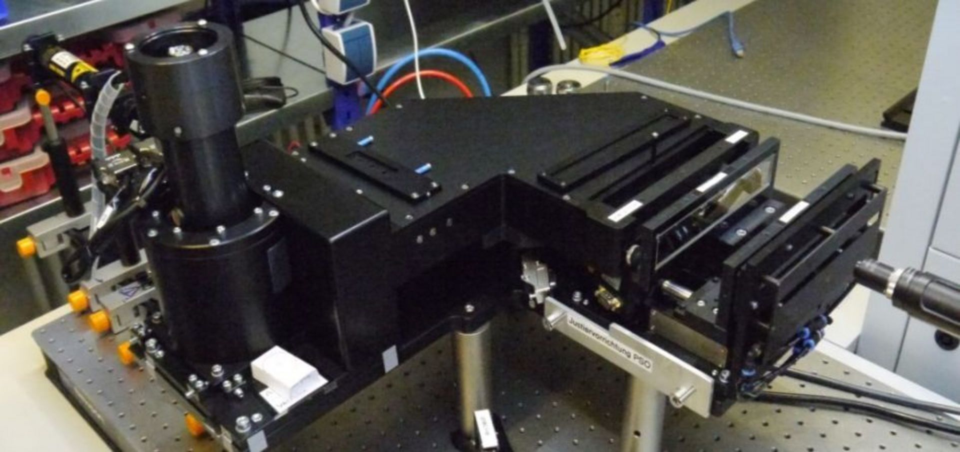
Setting up the performance test for the PSO assembly.
Picture: Ingeneric
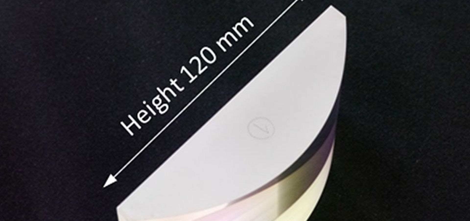
The large-format acylinders feature extreme aperture aspect ratios with a height of 120 millimeters and a length of 180 millimeters.
Picture: Ingeneric
Focus on a LED wafer
The concept envisaged splitting the light from a beam source into three separate beams and distributing it evenly over a scan length of 154 millimeters with a working distance of more than 40 millimeters. The goal was to make the focus smaller than ten micrometers while keeping the scan path deviation below two micrometers, all while maintaining a scanning linearity of less than one percent and a telecentricity error of less than one degree. Also on the to-do list was a variability in the angle of incidence of less than one degree and a zoom function of between 0.3 and two millimeters for the grid dimension between the parallel beams.
One approach that initially seemed very promising involved an anamorphic f-theta optics system with free form corrective optics. This corrected the scan line distortion but had a negative effect on beam focusability. That might have been acceptable in itself, but achieving the desired focal length also led to problems in compensating for the pyramidal error introduced by the polygon. Depending on the position of the beams on the target, this led to significant deviations that even free form optics can’t correct. What’s more, it proved impossible to achieve the desired grid spacings.
Acylinder as optics
Ingeneric changed tack and came to the conclusion that one optics system alone was incapable of fulfilling all the criteria. The team of developers therefore decided to accept some limitations in grid variability and working distance as the smallest deviation from the specifications.
But before the final concept could be implemented, there was still one more hurdle to overcome. One of the key components of the optics was not commercially available at the necessary level of quality at that time.
To implement rectangular scan fields of the required size and with the required large aspect ratio, the developers had planned to use an acylinder with a length of 180 millimeters as a “lens” in the optics system. At that time, however, the desired cutting accuracy of just a few micrometers posed requirements in regard to imaging accuracy that could be fulfilled only by microscopic acylinders that were just a few millimeters long.
Ingeneric therefore decided that the next step was to find a way of producing this kind of acylinder in-house. One of the key conditions was that whatever process they ended up with should have the potential to be scaled up to an industrial level. Otherwise this one piece of glass could end up jeopardizing the future economic viability of the entire cutting process.
The PSO in action
The completed PSO assembly passed its performance test on two test units with differently sized reproduction scales. The grid spacing, scanning linearity and scan path distortion were determined over the entire scan length in a 173-millimeter image field with a 9.0-micrometer resolution. The Focal spot size was assessed in different lateral and axial positions in an image field of 160 micrometers with a 0.4-micrometer resolution. The results confirmed that the optics system works with high precision. The optics also achieved this degree of precision in practical tests on optical LED wafers with a diameter of 6 millimeters.
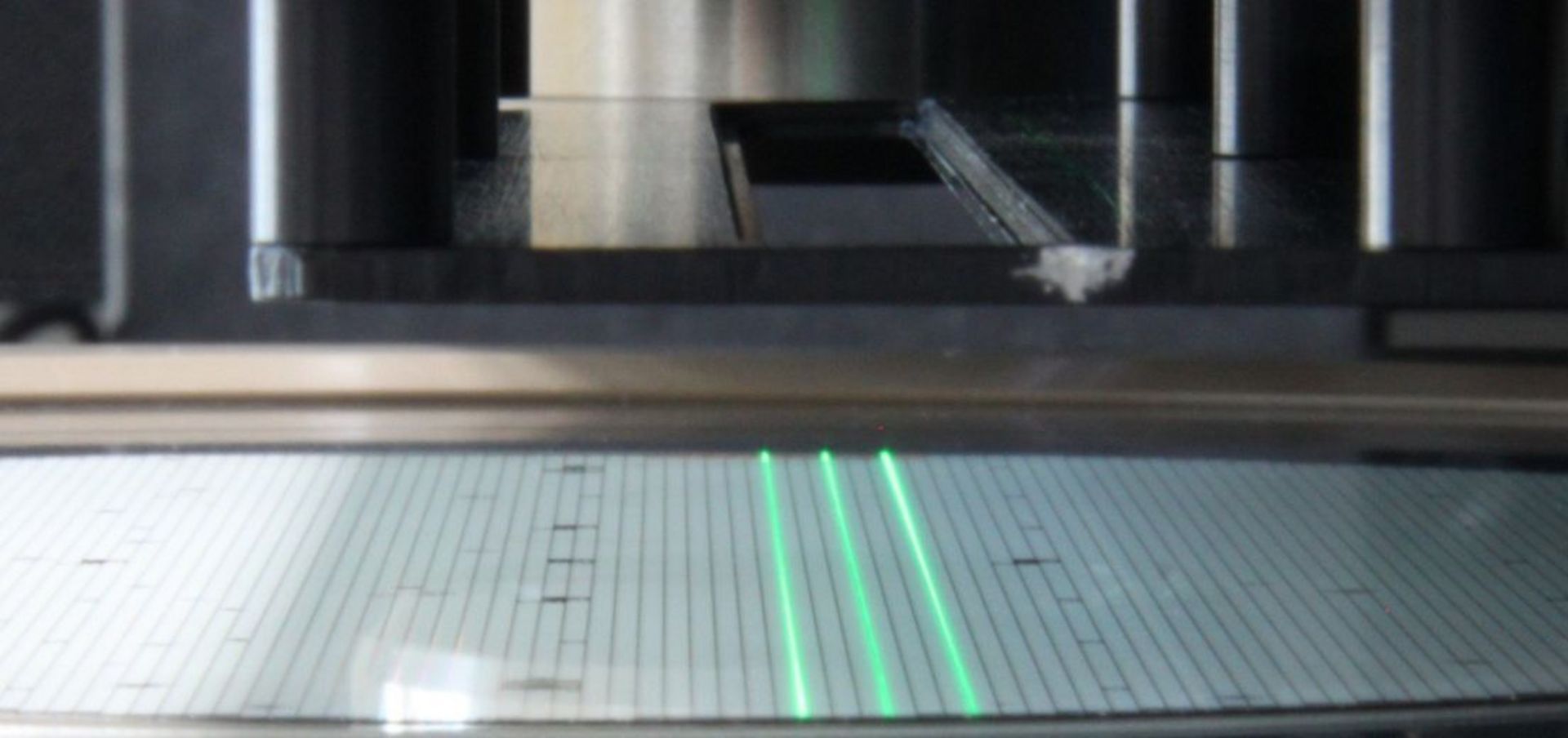
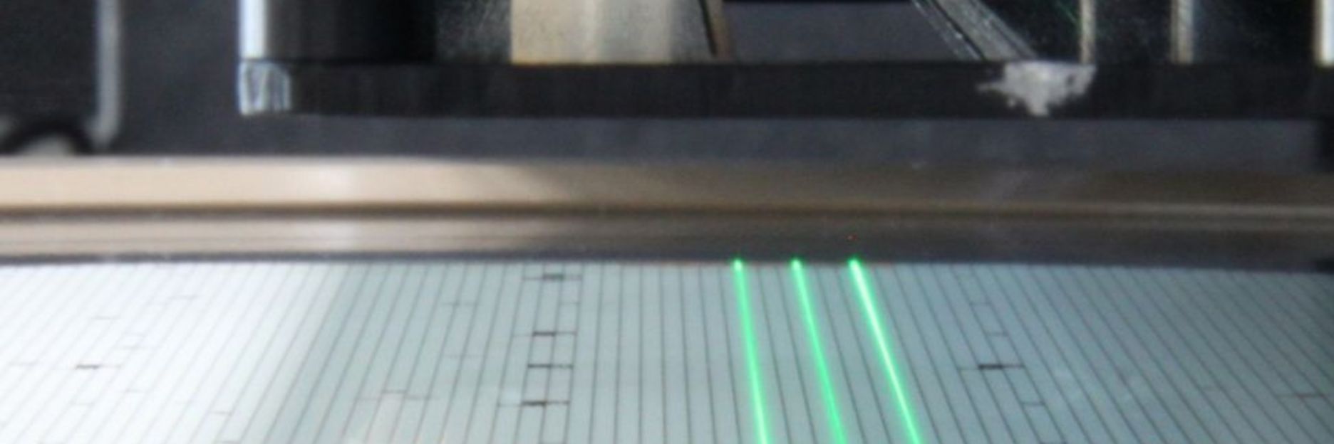
The light from the beam source is split into three separate beams and distributed evenly over a scan length of 154 millimeters with a working distance of more than 40 millimeters.
Picture: Osram
A basis for new developments
The Semilas project has now been completed, but only time will tell whether it actually results in a workable process. For a parallel process it will be essential – besides the qualitiy of optics – to generate ample power with the ultra-short pulsed laser in order to precisely distribute the pulse energy. However, as with all projects of this kind, much of the value of of Semilas stems from all the separate challenges that were successfully solved during the project. For example, the new method of constructing scanning optics with a large scan line opens up new possibilities when it comes to producing high-precision macroscopic acylinders. All in all, the project has paved the way to embark on new and even more sophisticated concepts with the reasonably confident assumption that lasers do indeed work “with extreme speed and precision”.
A prepared cylindrical blank is accurately attached to a carrier using optical cement. A zero point or hydraulic clamping system ensures there are no deviations in any of the subsequent grinding, polishing and measuring steps. The grinding process removes material transverse to the cylinder axis. It is particularly important in this process that the radius is maintained on the grinding wheel. In a final stage, CNC polishing is used to eliminate roughness peaks and damage to edge zones. The shape of the acylinder is gradually brought closer to the ideal contour by a process of periodic measuring, paring back the volume of material removal and repeating the polishing process.